PCB Back Drilling: When is it Necessary and How to Do it RightAuthor : Adrian September 13, 2025Table of ContentsIn the fast-paced world of electronics, maintaining signal integrity in high-speed printed circuit boards (PCBs) is a top priority for designers and engineers. One advanced technique that addresses this challenge is PCB back drilling. But when is back drilling necessary, and how can you ensure it’s done correctly? In this comprehensive guide, we’ll explore the essentials of back drilling, including when to use it, the detailed process, and best practices for via design and signal integrity. Whether you're optimizing a high-speed design or refining PCB design rules, this blog will provide actionable insights to help you achieve top performance.
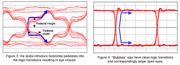
What is PCB Back Drilling and Why Does it Matter?PCB back drilling, also known as controlled depth drilling, is a manufacturing technique used to remove unused portions of copper from through-hole vias in a circuit board. These unused portions, often called "via stubs," can cause signal reflections and distortions in high-speed designs. By eliminating these stubs, back drilling enhances signal integrity, reduces noise, and ensures reliable performance in applications where data rates exceed 5 Gbps or even reach up to 25 Gbps in modern systems. Signal integrity is critical in industries like telecommunications, data centers, and aerospace, where even minor signal distortions can lead to data loss or system failures. Back drilling directly addresses these issues, making it an essential tool for engineers working on cutting-edge technology. In the following sections, we’ll dive into the specifics of when back drilling is necessary and how to implement it effectively.
When to Back Drill: Identifying the Need in Your PCB DesignBack drilling isn’t necessary for every PCB project. It’s a specialized process typically reserved for high-speed designs where signal integrity is paramount. Here are the key scenarios when you should consider back drilling:
However, back drilling isn’t always the answer. For low-speed designs or simpler two-layer boards where vias don’t pose a risk to signal quality, the added cost and complexity of back drilling may not be justified. A good rule of thumb is to simulate your design using signal integrity tools to determine if stubs will impact performance before deciding to back drill.
Understanding PCB Design Rules for Back DrillingIntegrating back drilling into your PCB design requires adherence to specific design rules to ensure manufacturability and performance. These rules help balance the technical needs of signal integrity with the practical constraints of manufacturing. Below are key PCB design rules to follow:
By incorporating these rules into your workflow, you can streamline the back drilling process and avoid costly redesigns or manufacturing defects. Always collaborate closely with your PCB manufacturer to confirm their capabilities and constraints before finalizing your design.
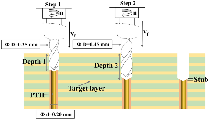
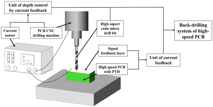
The Back Drilling Process: A Step-by-Step GuideThe back drilling process is a precise manufacturing technique that requires careful planning and execution. Here’s a detailed look at how it’s done, broken down into clear steps:
The precision of back drilling directly impacts its effectiveness. Errors in depth or alignment can compromise via functionality, so strict quality control is essential. Partnering with an experienced manufacturer ensures the process is executed flawlessly.
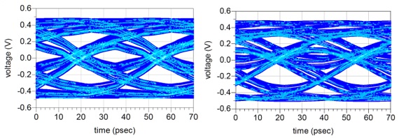
Signal Integrity Guide: How Back Drilling Improves PerformanceSignal integrity is the cornerstone of high-speed PCB design, and back drilling plays a pivotal role in achieving it. Here’s how this technique improves performance, along with practical tips for maximizing results:
To maximize signal integrity, combine back drilling with other techniques like proper layer stack-up design, controlled impedance routing, and differential pair matching. Use simulation tools early in the design phase to predict stub effects and prioritize which vias need back drilling.
Via Design Optimization: Best Practices for High-Speed PCBsEffective via design is critical to complement back drilling and ensure optimal signal integrity. Poorly designed vias can negate the benefits of back drilling, so follow these best practices for via design optimization:
Optimized via design, combined with back drilling, creates a robust foundation for high-speed PCBs. Always test prototypes to validate your design choices before moving to full-scale production.
Challenges and Limitations of Back DrillingWhile back drilling offers significant benefits, it’s not without challenges. Understanding these limitations helps you make informed decisions and plan accordingly:
Despite these challenges, the benefits of back drilling often outweigh the drawbacks for high-speed applications. Careful planning and collaboration with your manufacturing partner can mitigate most issues.
Conclusion: Mastering Back Drilling for Superior PCB PerformancePCB back drilling is a powerful technique for enhancing signal integrity in high-speed designs. By removing via stubs, it minimizes signal reflections, reduces crosstalk, and ensures reliable performance in critical applications. Knowing when to back drill—such as for data rates above 5 Gbps or multilayer boards with unused via portions—is the first step to leveraging this process effectively. Following PCB design rules, understanding the back drilling process, and optimizing via design further ensure success. For engineers and designers, mastering back drilling means balancing performance needs with manufacturing constraints. Use simulation tools to identify problem areas, adhere to precise design guidelines, and test prototypes to validate results. With these practices, you can achieve superior signal integrity and build PCBs that meet the demands of modern electronics. By integrating back drilling into your workflow, you’re not just solving a technical challenge—you’re future-proofing your designs for the ever-increasing speeds of tomorrow’s technology. Start applying these insights to your next project and see the difference in performance and reliability. Share · · · · The Role of Flux in PCB Wave Soldering: Selection, Application, and Residue RemovalMarch 16, 2026PCB wave soldering flux types include rosin, water-soluble, and no-clean options with varying activity levels for oxide removal and solder flow. This guide covers selection criteria, spray foam drop-jet application methods, residue removal processes, and alternatives like nitrogen blanketing to boost joint reliability and yields for engineers. Article Achieving Uniform Solder Fillets in PCB Wave Soldering: Process ControlMarch 16, 2026Achieve uniform solder fillets in PCB wave soldering with process control strategies. Optimize flux, preheat, wave height, conveyor speed for consistent fillet shape, height, and wetting balance. Includes visual inspection tips and troubleshooting for reliable through-hole assemblies. Boost quality in production. Article Optimizing Conveyor Speed for Efficient PCB Wave SolderingMarch 16, 2026Learn PCB wave soldering conveyor speed calculation to manage dwell time, immersion depth, and throughput effectively. Electric engineers get practical steps, best practices, and troubleshooting tips for higher process efficiency and fewer defects in wave soldering operations. Article Understanding IPC Standards for PCB Surface Finishes: Ensuring Quality and ComplianceMarch 11, 2026Understand IPC standards IPC 4552 ENIG and IPC 4553 immersion silver for PCB surface finishes. Ensure compliance, enhance solderability, and prevent common defects to achieve reliable, high quality circuit boards. Article Miniaturization Challenges in PCB AssemblyMarch 11, 2026Navigate the complexities of high density interconnect PCB assembly and precise component placement. Learn to tackle miniaturization challenges, from tiny part handling to thermal stress, ensuring robust and reliable electronics. Article High Speed Routing Techniques: PCBMarch 11, 2026Master high speed routing in PCBs to ensure signal integrity and minimize electromagnetic interference. Learn essential techniques for robust designs, from controlled impedance to differential pair strategies. Prevent performance issues and achieve reliable electronics. ArticleGet Instant PCB |